Last Updated on 14 10 月, 2025 by

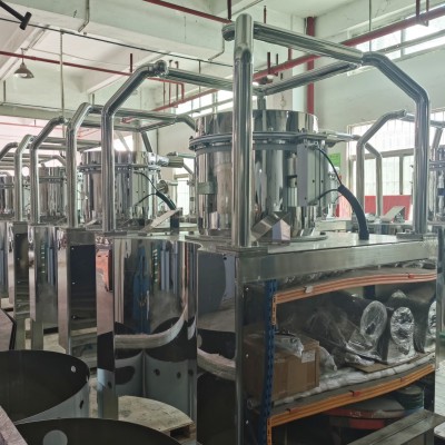
In the nano-scale world of chip manufacturing, equipment frames and bases form the “lifeline” of lithography scanners, etch chambers, and CVD reactors. Where <1μm vibration errors impact yield, and metal ion release contaminates EUV optics, only aerospace-grade stainless steel and molecular-level cleanliness can safeguard chip fabrication. We specialize in mission-critical structural components with zero distortion, zero outgassing, and zero magnetic interference for 3nm node resilience.
I. Semiconductor “Foundation” Challenges
| Critical Risk | Threshold | Our Countermeasure |
|---|---|---|
| Micro-Vibration | >5nm @100Hz | Hybrid damping + honeycomb ribs |
| Thermal Drift | ΔL>0.1μm/°C | CTE-matched design (≤9.5×10⁻⁶/K) |
| Metal Contamination | >0.1 particles/cm²·min | EP + scCO₂ cleaning |
| Residual Magnetism | μr>1.002 | Non-magnetic steel (μr<1.0005) |
| Wafer-Level Flatness | >0.02mm/m² | Stress relief + nano-scraping |
II. Core Technologies: Redefining Standards
-
Material Genomics
-
Ultra-low gas steel: 316L VIM-VAR
✓ [O]<30ppm | [S]<0.001% | [H]<1.5ppm -
Specialty alloys:
▶ Non-magnetic high-Mn steel (etch gas resistance)
▶ Invar® (zero CTE)
▶ Hastelloy® C-22 (HF vapor resistance)
-
-
Nanoscale Surface Engineering
Process Chain:
[Vibration aging] → [Cryo-stabilization] → [Precision grinding (0.01mm/m²)] → [Ion beam figuring (±0.1μm)]-
Vacuum reference surface: ≤3μm/Φ600mm
-
Mounting hole accuracy: ±5μm position, 0.005mm/100mm perpendicularity
-
-
Zero-Distortion Welding
-
Laser cold welding: Heat input <8J/mm, HAZ<100μm
-
EB vacuum welding: 20:1 depth-to-width, distortion<0.01%
-
Post-weld treatment:
✓ TIG remelting (porosity elimination)
✓ Shot peening (fatigue resistance)
✓ EP (Ra≤0.1μm)
-
-
Molecular-Level Cleanliness
Process Key Metric Standard Electro-polishing Ra≤0.08μm SEMI F19 Passivation Cr₂O₃ ≥15nm AES analysis scCO₂ cleaning Hydrocarbons <0.1μg/cm² TOF-SIMS SiOx coating Surface resistivity >10¹⁵Ω ESD S20.20 -
Extreme Validation
-
Vibration: SEMI S23/M1.8 compliant (0.1–500Hz)
-
Outgassing: TDS analysis <5×10⁻¹⁰ torr·L/(s·cm²)
-
Cleanliness: ISO 14644-1 Class 3
-
Magnetic shielding: <0.2 Gauss (10mm distance)
-
III. Advanced Node Solutions
| Application | Challenge | Our Innovation |
|---|---|---|
| EUV Lithography Base | Thermal drift <0.5nm/mm² | Microchannel cooling + Invar® inserts |
| ALD Reaction Disk | Cl₂/HF corrosion resistance | Nitrided Hastelloy® C-22 surface |
| Ion Implant Yoke | Zero magnetism + rigidity | Ceramic-stainless composite |
| Wafer Robot Arm | Specific stiffness >40GPa/(g/cm³) | Topology-optimized honeycomb |
IV. Why Global Fabs Choose Us
-
Digital Twin Manufacturing:
✓ ANSYS multiphysics simulation (thermal-structural-vibration)
✓ <3% weld distortion prediction error -
Certification Stack:
▶ SEMI F47 (voltage sag immunity)
▶ ISO 14644 Class 3
▶ NASA STD 6002 (outgassing) -
Full Traceability:
✓ Material traceability to melt batch
✓ 20-year process video archive -
Global Rapid Response:
▶ 48h DFM reports
▶ Localized support (Asia/Europe/Americas)
V. Military-Grade Workflow
-
Requirements Lock: Interface drawings/operational profiles (vibration spectra, corrosives, thermal cycles)
-
Virtual Prototyping: Simulation report + FMEA
-
Execution: Live cleanroom monitoring
-
Packaging: Class 10 vacuum-sealed
-
Delivery Dossier:
-
Full metrology report (CMM + laser tracker)
-
Material certs (composition/metallurgy/IGC)
-
Semiconductor Structural Component Installation Protocol
-
Precision Foundation. Nanoscale Integrity.
When 0.01°C thermal drift defocuses EUV lenses or 1ng metal contamination ruins wafers, we deliver atomic-scale material control, sub-nanometer accuracy, and molecular cleanliness—forging the steel backbone of chipmaking.


